Facing the crucial challenges for our society -such assustainable development, health, information technologies- requires the ability to imagine and create advanced materials with innovative properties controlling their composition, structure and morphology at the micro and nanoscale. The combination of different nano-systems in fact opens up a new world to explore, with properties and phenomena that are not the simple sum of those of individual objects, with possibilities for completely new applications. The application areas of these systems range from catalysis, photovoltaics and tribology to those inherent in ICT developments, such as nano-electronics, spin- and opto-electronics, nano-mechanics and new quantum technologies.
The activities at FIM are focused on:
- Nanofabrication
Electron-beam lithography and FIB
On-surface synthesis
Nanoparticle physical deposition - Tribology and nanomechanics
Graphene and 2D materials
Multiscale surface modifications
Hard coatings and self-lubricants - Surface spectroscopies and microscopies
Oxide films, nanostructures and nanoparticles for sustainable energy solutions
Graphene nanostructures and 2D metal-dichalcogenides systems
Hybrid molecular magnets/inorganic substrate interfaces - Transmission Electron Microscopy spectroscopy and diffraction
Electron Holography of magnetic materials and electromagnetic fields
Orbital angular momentum (OAM) resolved /EELS
Basic experiment in quantum mechanics exploiting the TEM
Faculty
Marco Affronte, Antonio Ballestrazzi, Marco Beleggia, Roberto Biagi, Giuseppe Cantarella, Sergio D’Addato, Valentina De Renzi, Stefano Frabboni, Claudia Menozzi, Francesco Rossella, Alberto Rota, Elisabetta Salerno, Rita Tonini, Sergio Valeri

Nanomaterials can be fabricated using two different approaches, i.e. top-down and bottom-up. Top-down nanofabrication makes nano-structures by repeated use of additive (film deposition) and subtractive steps that take parts of them away, while the bottom-up approach exploits the self-assembling properties of matter to obtain precisely defined nanosystems.
At FIM, the top-down approach is used to fabricate devices and systems for nanomagnetism, nanophotonics, diffractive optics and electron optics, tribology and more. Example in the field are:
- Nanofabrication and characterization of hybrid nanodevices for (spin/opto) electronics.
- Nanofabrication of electron-optical devices for electron beam shaping and detection.
- Surface patterning for tribological studies.
Moreover, examples of bottom-up nanofabrication at FIM are:
- Physical deposition of metal and oxide nanoparticles (2-10 nm diameter) with applications in photocatalysts, solid state fuel cells and photovoltaic devices.
- on surface synthesis of atomically-precise, ultranarrow graphene nanoribbons.
Image adapted from J. Phys. Chem. C 121, 10620 (2017)
People: Prof. M. Affronte, Prof. M. Beleggia, Prof. R. Biagi, Prof. S. D’Addato, Prof. V. De Renzi, Prof. S. Frabboni, Prof. Rossella, Dr. G. Cantarella, Dr. C. Menozzi, Dr. R. Tonini; Dr A. di Bona (CNR), Dr. G. Gazzadi (CNR)

Tribological phenomena play a key role in all mechanical systems where interacting surfaces are in relative motion, consuming energy and raw materials, producing CO2 and other contaminants. It is then strategic to study the tribological processes --friction, lubrication and wear--, with the aim of understanding fundamental phenomena and developing novel solutions for industrial applications.
The main topics of SUP&RMAN laboratory at FIM are:
- Graphene and 2D materials for tribological applications
- Multiscale surface modifications for the control of friction, wear and wettability
- Hard coatings and self-lubricant coatings for the reduction of friction, wear and corrosion
We address basic research as well as applied research and technology transfer, often in collaboration with local and national companies interested in developing new high-performance and low-impact products.
Image adapted from J. Nanosci. Nanotechnol. 11, 9260 (2011).
People: Dr. A. Ballestrazzi, Dr. A. Rota, Prof. S. Valeri; Dr. G. Paolicelli (CNR)
Novel nanostructured and low-dimensional systems are of keys interes for ICT applications, as well as for promising cost-effective and sustainable energy solutions. Examples of such systems comprise:
- oxide films, nanostructures and nanoparticles, with application in photocatalysts, fuel cells, and third-generation photovoltaic devices;
- atomically-precise graphene nanostructures and 2D metal-dichalcogenides systems, which display novel and intriguing electronic and optical properties; -
- hybrid molecular magnets/inorganic substrate interfaces.
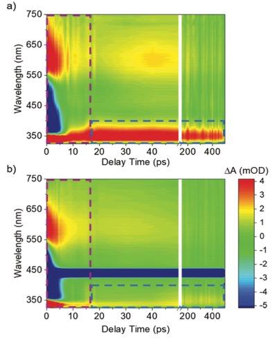
At FIM, advanced spectroscopies and scanning microscopies (STM, AFM) are exploited - both on campus and at synchrotron radiation and free-electron laser facilities – for a thorough characterization of the nanoscale properties of such materials. Among the available on-campus techniques, high-resolution electron energy loss spectroscopy represents a powerful tool to investigate both localized vibrational modes and collective excitation (phonon, plasmon, excitons) dispersions. Moreover, pump-probe spectroscopies - performed with shared table top ultrafast laser facilities (SPRINT Trieste and EFSL Roma) and with the free electron laser FERMI at the ELETTRA laboratories in Trieste - allow us to investigate the transient mechanisms at the base of photocatalysis and photovoltaic effects, down to femtosecond time scales.
Images adapted from Nanoscale 12, 19681 (2020) and Nanoscale 11, 10282 (2019).
People: Prof. M. Beleggia, Prof. R. Biagi, Prof. S. D’Addato, Prof. V. De Renzi; Dr. A. di Bona (CNR), Dr. P. Luches (CNR), Dr. S. Benedetti (CNR)

Transmission electron microscopy (TEM/STEM) is an effective tool for the analysis of crystal structure elemental/chemical-bonding and magnetic domain structure with a high spatial resolution. One of our goals is to develop/improve various advanced electron microscopy methods like scanning transmission electron microscopy (STEM), electron energy-loss spectroscopy (EELS), Electron diffraction, Holography and Lorentz microscopy for the analysis of nanostructures. We also exploit the electron microscope as a tool for the realization of basic experiments in quantum mechanics:
- Electron Holography of magnetic materials and electromagnetic fields
- Orbital angular momentum (OAM) resolved /EELS: high spatial resolution Electron Magnetic dichroism and plasmonics;
- Basic experiment in quantum mechanics exploiting the Transmission Electron Microscope.
Main collaborations: Ernst Ruska-Centre for Microscopy and Spectroscopy with Electrons and Peter Grünberg Institute, Forschungzentrum Jülich, Germany.
Images adapted from Sci. Rep. 9, 10458 (2019) and Phys Rev. B 100, 224409 (2019).
People : Prof. M. Beleggia, Prof. S. Frabboni, Dr. C. Menozzi; Dr. G. Gazzadi (CNR), Dr. V. Grlllo (CNR)